SpecificationsItem Name: LED DRIVERInput: 90 to 300 VAC ; 47 - 53 Hz, L N EOutput: WITH POWER FACTOR CORRECTION50V@0.7APower factor & THD: 0.99 & 8-10%Line and Load Regulation:1 %Output Ripple: 1 %,Operating Temperature:-10 to 50 deg C ; RH 95 % non condensingOutput Isolation: 1.5 KV rms @ 50 Hz for 1 minute.Other Features: • Output over voltage protection • Input EMI-RFI filters• Output LED indication • Integrated MOSFET and PFcontrollersfor greater reliability and space savingEfficiency:>85 % at full load and normal I/PStand by power:<100mWOutput variation: Apprx. ±1%IF U WOULD LIKE TO DESIGN THIS PRODUCT THAN CALL ME :9716933131OR MAIL ME:kaushal.talk@gmail.com
Friday, December 23, 2011
35W LED DRIVER THD < 10percent
Thursday, August 18, 2011
260W battery charger solution low cost

Specifications
Of
13.5Volt@20Amp.
Input: 170 to 300 VAC ; 47 - 53 Hz, L N E
Output: 13.5V@20A
function:
INPUT UNDER VOLTAGE CUT OFF AT 145VAC
OVER VOLTAGE SHUT DOWN AT 310VAC
BATTERY REVERSE PROTECTION
Line and Load Regulation: 1 %
Output Ripple: 1 %,
Operating Temperature: 10 to 50 deg C ; RH 95 % non condensing
Output Isolation: 1.8 KV rms @ 50 Hz for 1 minute.
Other Features: Output short circuit protection • Input EMI-RFI filters •
• Integrated MOSFET and PWM controllers for greater reliability and space saving.;
IF U WOULD LIKE TO DESIGN THIS PRODUCT THAN CALL ME :+919716933131OR MAIL ME:kaushal.talk@gmail.com
Tuesday, August 16, 2011
POWER SUPPLY UNIT 5V @10AMP.

Specifications
Of
Item Name: SMPS 5V @ 10A
Input: 170 to 265 VAC ; 47 - 53 Hz, L N E
Output: 5 V @ 10A
Line and Load Regulation: 1 %
Output Ripple: 1 %,
Operating Temperature: -10 to 50 deg C ; RH 95 % non condensing
Output Isolation: 1.5 KV rms @ 50 Hz for 1 minute.
Other Features: Input over voltage latch protection • Output over voltage latch protection
• Output short circuit protection • Input EMI-RFI filters
• Screw type input / output connectors 2+2 • Output LED indication
• Integrated MOSFET and PWM controllers for greater reliability and space saving
Efficiency: >77 % at full load and normal I/P
Stand by power: <3.6W
Output variation: Apprx. ±5% through preset.
IF U WANT TO DESIGN THIS PRODUCT THAN CALL ME :+919716933131
OR MAIL ME:kaushal.talk@gmail.com
Tuesday, August 9, 2011
260 WATT BATTERY CHARGER SOLUTION:

Specifications
Of
13.5Volt@20Amp.
Input: 170 to 300 VAC ; 47 - 53 Hz, L N E
Output: 13.5V@20A
function:
INPUT UNDER VOLTAGE CUT OFF AT 145VAC
OVER VOLTAGE SHUT DOWN AT 310VAC
BATTERY REVERSE PROTECTION
Line and Load Regulation: 1 %
Output Ripple: 1 %,
Operating Temperature: 10 to 50 deg C ; RH 95 % non condensing
Output Isolation: 1.8 KV rms @ 50 Hz for 1 minute.
Other Features: Output short circuit protection • Input EMI-RFI filters •
• Integrated MOSFET and PWM controllers for greater reliability and space saving.;
IF U WOULD LIKE TO DESIGN THIS PRODUCT THAN CALL ME :+919716933131OR MAIL ME:kaushal.talk@gmail.com
Monday, August 1, 2011
80 watt led driver solution

Specifications
Item Name: SMPS 170V @ 0.53A
Input: 90 to 300 VAC ; 47 - 53 Hz, L N E
Output: 170 V @ 0.53 A WITH POWER FACTOR CORRECTION
Power factor & THD: >0.95 & 8-12%
Line and Load Regulation: 1 %
Output Ripple: 1 %,
Operating Temperature:-10 to 50 deg C ; RH 95 % non condensing
Output Isolation: 1.5 KV rms @ 50 Hz for 1 minute.
Other Features: • Output over voltage protection • Output short circuit protection
• Input EMI-RFI filters • Screw type input / output connectors • Output LED indication
• Integrated MOSFET and PWM controllers for greater reliability and space saving Option for over heat management
Efficiency: >85 % at full load and normal I/P
Output current variation: Approx. ±5%
IF U WOULD LIKE TO DESIGN THIS PRODUCT THAN CALL ME :9716933131
OR MAIL ME:kaushal.talk@gmail.com
Sunday, July 31, 2011
8WATT LED DRIVER SOLUTIION

Specifications
Item Name: LED DRIVER
Input: 90 to 300 VAC ; 47 - 53 Hz, L N E
Output: WITH POWER FACTOR CORRECTION
16V@0.7A
Power factor & THD: 0.99 & 8-16%
Line and Load Regulation:1 %
Output Ripple: 1 %,
Operating Temperature:-10 to 50 deg C ; RH 95 % non condensing
Output Isolation: 1.5 KV rms @ 50 Hz for 1 minute.
Other Features: • Output over voltage protection • Input EMI-RFI filters
• Output LED indication • Integrated MOSFET and PFcontrollers
for greater reliability and space saving
Efficiency:>85 % at full load and normal I/P
Stand by power:<100mW
Output variation: Apprx. ±1%
IF U WOULD LIKE TO DESIGN THIS PRODUCT THAN CALL ME :9716933131
OR MAIL ME:kaushal.talk@gmail.com
25 WATT LED DRIVER SOLUTION

Specifications
Item Name: LED DRIVER
Input: 90 to 300 VAC ; 47 - 53 Hz, L N E
Output: WITH POWER FACTOR CORRECTION
90V@0.35A
Power factor & THD: 0.99 & 8-16%
Line and Load Regulation:1 %
Output Ripple: 1 %,
Operating Temperature:-10 to 50 deg C ; RH 95 % non condensing
Output Isolation: 1.5 KV rms @ 50 Hz for 1 minute.
Other Features: • Output over voltage protection • Input EMI-RFI filters
• Output LED indication • Integrated MOSFET and PFcontrollers
for greater reliability and space saving
Efficiency:>85 % at full load and normal I/P
Stand by power:<100mW
Output variation: Apprx. ±1%
IF U WOULD LIKE TO DESIGN THIS PRODUCT THAN CALL ME :9716933131
OR MAIL ME:kaushal.talk@gmail.com
20 WATT LED DRIVER SOLUTION

Specifications
Item Name: 20 WATT LED DRIVER
Input: 90 to 300 VAC ; 47 - 53 Hz, L N E
Output: WITH POWER FACTOR CORRECTION
40V@0.7A
Power factor & THD: 0.99 & 8-16%
Line and Load Regulation:1 %
Output Ripple: 1 %,
Operating Temperature:-10 to 50 deg C ; RH 95 % non condensing
Output Isolation: 1.5 KV rms @ 50 Hz for 1 minute.
Other Features: • Output over voltage protection • Input EMI-RFI filters
• Output LED indication • Integrated MOSFET and PFcontrollers
for greater reliability and space saving
Efficiency:>85 % at full load and normal I/P
Stand by power:<100mW
Output variation: Apprx. ±1%
IF U WOULD LIKE TO DESIGN THIS PRODUCT THAN CALL ME :9716933131
OR MAIL ME:kaushal.talk@gmail.com
35WATT LED DRIVER SOLUTION

Specifications
Item Name:SMPS 54V @ 0.7A
Input:90 to 300 VAC ; 47 - 53 Hz, L N E
Output:54 V @ 0.7 A WITH POWER FACTOR CORRECTION
Power factor & THD:0.9999 & 8-16%
Line and Load Regulation:1 %
Output Ripple:1 %,
Operating Temperature:-10 to 50 deg C ; RH 95 % non condensing
Output Isolation: 1.5 KV rms @ 50 Hz for 1 minute.
Other Features: • Output over voltage protection • Output short circuit protection
• Input EMI-RFI filters • Screw type input / output connectors • Output LED indication
• Integrated MOSFET and PWM controllers for greater reliability and space saving.
Efficiency:>85 % at full load and normal I/P
Stand by power:<100mW
Output variation:Apprx. ±1%
IF U WOULD LIKE TO DESIGN THIS PRODUCT THAN CALL ME :9716933131
OR MAIL ME:kaushal.talk@gmail.com
Saturday, July 30, 2011
65 WATT LED DRIVER SOLUTION

Specifications
Item Name: SMPS 85V @ 0.7A
Input: 90 to 300 VAC ; 47 - 53 Hz, L N E
Output: 85 V @ 0.7 A WITH POWER FACTOR CORRECTION
Power factor & THD: >0.95 & 8-12%
Line and Load Regulation: 1 %
Output Ripple: 1 %,
Operating Temperature:-10 to 50 deg C ; RH 95 % non condensing
Output Isolation: 1.5 KV rms @ 50 Hz for 1 minute.
Other Features: • Output over voltage protection • Output short circuit protection
• Input EMI-RFI filters • Screw type input / output connectors • Output LED indication
• Integrated MOSFET and PWM controllers for greater reliability and space saving Option for PWM dimming the LED
Efficiency: >85 % at full load and normal I/P
Output current variation: Approx. ±5%
IF U WOULD LIKE TO DESIGN THIS PRODUCT THAN CALL ME :9716933131
OR MAIL ME:kaushal.talk@gmail.com
Sunday, July 24, 2011
SMPS 5V@5A 25 watt solution:
Specification’s
of
SMPS 5V @ 5A
you can manufacture, switched-mode power supply
(SMPS) (SMPS 5V @ 5A) is an electronic power
supply unit (PSU) that incorporates a switching
=>regulator. The salient features are enlisted below:
=>Input: 170 to 300 VAC ; 47 - 53 Hz, 3 wire
=>Output: 5 V @ 5 A
=>Line and Load Regulation: 1 %
=>Output Ripple: 1 %,
=>Operating Temperature: -10 to 50 deg C ; RH 95 % non condensing
=>Output Isolation: 1.5 KV rms @ 50 Hz for 1 minute.
=>Other Features: Input over voltage latch protection • Output over
voltage latch protection • Over temperature protection
• Output short circuit protection • Input EMI-RFI
filters • Screw type input / output connectors • Output
LED indication • Integrated MOSFET and PWM
controllers for greater reliability and space saving
=>Efficiency: >77 % at full load and normal I/P
=>Stand by power: <0.2W
=>Output variation: Approx. ±5% through preset.
 |
| 25 watt power supply schematic : |
I will make easy for u:
 |
| list of material :1 |
 |
| list of material:2 |
 |
| transformer design: for 5volt @5amp. |
Testing procedure
for
for
5volt @5amp.
1. Turn the output voltage adjustment preset to maximum. Connect to
normal input voltage and turn on the SMPS to check if it shuts down.
It should not shut down.
2. Adjust preset for rated output voltage.
3. Load the SMPS for rated full load.
4. Vary the AC input supply by variac from 170 to 300VAC and note if
there is any major change in output voltage.
5. Increase input voltage greater than 300VAC to check line overvoltage
shutdown.
6. Measure Drain voltage of device. At 420VDC input it should be a
maximum of 630V.
7. Check the input voltage at which the SMPS shuts down and gets
latched (input over voltage latching shutdown). It should be less than
440 volts.
8. Check the output voltage at which the SMPS shuts down and gets
latched (output over voltage latching shutdown). It should be greater
than the maximum adjustment limit of output adjustment preset.
9. Perform a High-voltage test of 1.5KV for 1 minute –
a. Between Input and Output.
b. Between Input and Earth.
 |
| PCB layout guideline |
thanks
kaushalesh singh(9716933131)
Thursday, July 14, 2011
12 WATT SMPS SOLUTION
Specifications
Of
Item Name: SMPS 12V @ 1A
Item Code: 09A
switched-mode power supply (SMPS) (SMPS 12V @ 1A) is an electronic power supply unit (PSU) that incorporates a switching regulator. The salient features are enlisted below:
Input: 170 to 265 VAC ; 47 - 53 Hz, L N
Output: 12V @ 1A
Line and Load Regulation: 1 %
Output Ripple: 1%,
Operating Temperature: -10 to 50 deg C ; RH 95 % non condensing
Output Isolation: 1.5 KV rms @ 50 Hz for 1 minute.
Other Features:
Output short circuit protection • Input EMI-RFI filters • Screw type input / output connectors • Output LED indication • Integrated MOSFET and PWM controllers for greater reliability and space saving
Efficiency: >74 % at full load and normal I/P
Stand by power: <1.12
Output variation: Apprx. ±5% through preset.
TESTING PROCEDURE:
RATING: I/P:170V~265VAC, O/P: 12V--1A
A) VISUAL CHECKING
CHECK DRY SOLDERING CHECK POLARITY OF COMPONENT.
B) ELECTRICAL TEST
1. Connect the input and output, make sure the Line Neutral Earth at CN1 is OK and +Ve, -Ve at output is proper on your zic without Load and adjust the variac for 170V.
2. Switch on the psu and see the operation as follows:
(a). Bulb in series with a little glow.
(b). Output voltmeter show voltage 12V ±1%.
(c). If the AC ampere meter is on your zic, check the current in mA is showing.
(d). Output LED indication is Green.
3. Bypass the bulb and increase the load gradually to the maximum (1A) [make sure that your load resistance is proper] see the voltage regulation is ok (±1% is recommended) and increase the input voltage up to 265Vac and confirm that line regulation is maintaining [±1% recommended ].
4. Switch ON and OFF the power supply many times with full load, both at low ac input [170V] and high ac input[265V]. make sure every time working properly.
5.Increase the Ac volt up to 280v and see the shutdown in between 280v and 290v and Decrease the voltage 265V and see restarting.
Of
Item Name: SMPS 12V @ 1A
Item Code: 09A
switched-mode power supply (SMPS) (SMPS 12V @ 1A) is an electronic power supply unit (PSU) that incorporates a switching regulator. The salient features are enlisted below:
Input: 170 to 265 VAC ; 47 - 53 Hz, L N
Output: 12V @ 1A
Line and Load Regulation: 1 %
Output Ripple: 1%,
Operating Temperature: -10 to 50 deg C ; RH 95 % non condensing
Output Isolation: 1.5 KV rms @ 50 Hz for 1 minute.
Other Features:
Output short circuit protection • Input EMI-RFI filters • Screw type input / output connectors • Output LED indication • Integrated MOSFET and PWM controllers for greater reliability and space saving
Efficiency: >74 % at full load and normal I/P
Stand by power: <1.12
Output variation: Apprx. ±5% through preset.
 | ||
| SCHEMATIC FOR 12V 1A |

 |
| COMPONENT DETAIL |
 |
| TRANSFORMER DETAIL'S |
 | |
| PCB DRAWING |
RATING: I/P:170V~265VAC, O/P: 12V--1A
A) VISUAL CHECKING
CHECK DRY SOLDERING CHECK POLARITY OF COMPONENT.
B) ELECTRICAL TEST
1. Connect the input and output, make sure the Line Neutral Earth at CN1 is OK and +Ve, -Ve at output is proper on your zic without Load and adjust the variac for 170V.
2. Switch on the psu and see the operation as follows:
(a). Bulb in series with a little glow.
(b). Output voltmeter show voltage 12V ±1%.
(c). If the AC ampere meter is on your zic, check the current in mA is showing.
(d). Output LED indication is Green.
3. Bypass the bulb and increase the load gradually to the maximum (1A) [make sure that your load resistance is proper] see the voltage regulation is ok (±1% is recommended) and increase the input voltage up to 265Vac and confirm that line regulation is maintaining [±1% recommended ].
4. Switch ON and OFF the power supply many times with full load, both at low ac input [170V] and high ac input[265V]. make sure every time working properly.
5.Increase the Ac volt up to 280v and see the shutdown in between 280v and 290v and Decrease the voltage 265V and see restarting.
Thursday, June 30, 2011
Thevenin’s Theorem:
Thevenin’s Theorem
There are times when it is advantageous to isolate a part of the circuit to simplify the analysis of the isolated part of the circuit. Rather than write loop or node equations for the complete circuit, and solving them simultaneously, Thevenin’s theorem enables us to isolate the part of the circuit we are interested in. We then replace the remaining circuit with a simple series equivalent circuit, thus Thevenin’s theorem simplifies the analysis.
There are two theorems that do similar functions. The Thevenin theorem just described
is the first, and the second is called Norton’s theorem. Thevenin’s theorem is used when
the input source is a voltage source, and Norton’s theorem is used when the input source
is a current source. Norton’s theorem is rarely used, so its explanation is left for the reader to dig out of a textbook if it is ever required.The rules for Thevenin’s theorem start with the component or part of the circuit being replaced.Referring to Figure 2–7, look back into the terminals (left from C and R3 toward
point XX in the figure) of the circuit being replaced. Calculate the no load voltage (VTH)as seen from these terminals (use the voltage divider rule).

Look into the terminals of the circuit being replaced, short independent voltage sources,and calculate the impedance between these terminals. The final step is to substitute theThevenin equivalent circuit for the part you wanted to replace as shown in Figure 2–8.

The Thevenin equivalent circuit is a simple series circuit, thus further calculations are simplified.
The simplification of circuit calculations is often sufficient reason to use Thevenin’s theorem because it eliminates the need for solving several simultaneous equations. The detailed information about what happens in the circuit that was replaced is not available when using Thevenin’s theorem, but that is no consequence because you had no interest in it.
As an example of Thevenin’s theorem, let’s calculate the output voltage (VOUT) shown in Figure 2–9A. The first step is to stand on the terminals X–Y with your back to the output circuit, and calculate the open circuit voltage seen (VTH). This is a perfect opportunity to use the voltage divider rule to obtain Equation 2–13.

Still standing on the terminals X-Y, step two is to calculate the impedance seen looking into these terminals (short the voltage sources). The Thevenin impedance is the parallel impedance of R1 and R2 as calculated in Equation 2–14. Now get off the terminals X-Y before you damage them with your big feet. Step three replaces the circuit to the left of X-Y with the Thevenin equivalent circuit VTH and RTH.

The final step is to calculate the output voltage. Notice the voltage divider rule is used again. Equation 2–15 describes the output voltage, and it comes out naturally in the form of a series of voltage dividers, which makes sense. That’s another advantage of the voltage divider rule; the answers normally come out in a recognizable form rather than a jumble of coefficients and parameters.
Monday, June 27, 2011
Law of physics:
Law of physics:
Ohm’s law is stated as V=IR and it is fundamental to all electronics. Ohm’s law can be applied to a single component, to any group of components, or to a complete circuit. When the current flowing through any portion of a circuit is known, the voltage dropped across that portion of the circuit is obtained by multiplying the current times the resistance (Equation 2–1).
V=IR
In Figure 2–1, Ohm’s law is applied to the total circuit. The current, (I) flows through the total resistance (R), and the voltage (V) is dropped across R.

In Figure 2–2, Ohm’s law is applied to a single component. The current (IR) flows through the resistor (R) and the voltage (VR) is dropped across R. Notice, the same formula is used to calculate the voltage drop across R even though it is only a part of the circuit.

Kirchoff’s voltage law states that the sum of the voltage drops in a series circuit equals
the sum of the voltage sources. Otherwise, the source (or sources) voltage must be
dropped across the passive components. When taking sums keep in mind that the sum
is an algebraic quantity. Kirchoff’s voltage law is illustrated in Figure 2–3 and Equations
2–2 and 2–3.
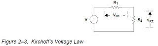
Vsources =Vdrops.
V=Vr1+Vr2.
Kirchoff’s current law states: the sum of the currents entering a junction equals the sum
of the currents leaving a junction. It makes no difference if a current flows from a current source, through a component, or through a wire, because all currents are treated identically. Kirchoff’s current law is illustrated in Figure 2–4 and Equations 2–4 and 2–5.

Iin=Iout.
I1+I2=I3+I4.
Voltage Devider Rule:
When the output of a circuit is not loaded, the voltage divider rule can be used to calculate the circuit’s output voltage. Assume that the same current flows through all circuit elements (Figure 2–5). Equation 2–6 is written using Ohm’s law as V = I (R1 + R2). Equation –7 is written as Ohm’s law across the output resistor.

I =V / (R1+R2)
Vout= I R2
Vout=VR2 / (R1+R2)
A simple way to remember the voltage divider rule is that the output resistor is divided by
the total circuit resistance. This fraction is multiplied by the input voltage to obtain the out-put voltage. Remember that the voltage divider rule always assumes that the output resistor is not loaded; the equation is not valid when the output resistor is loaded by a parallel component. Fortunately, most circuits following a voltage divider are input circuits, and input circuits are usually high resistance circuits. When a fixed load is in parallel with the output resistor, the equivalent parallel value comprised of the output resistor and loading resistor can be used in the voltage divider calculations with no error. Many people ignore the load resistor if it is ten times greater than the output resistor value, but this calculation can lead to a 10% error.
CURRENT DIVIDER RULE:
When the output of a circuit is not loaded, the current divider rule can be used to calculate the current flow in the output branch circuit (R2). The currents I1 and I2 in Figure 2–6 are assumed to be flowing in the branch circuits. Equation 2–9 is written with the aid of Kirchoff’s current law. The circuit voltage is written in Equation 2–10 with the aid of Ohm’s law. Combining Equations 2–9 and 2–10 yields Equation 2–11.

Figure 2–6. Current Divider Rule
I=I1+I2
V=I1R1=I2R2
I=I1+I2=I2(R2/R1)+I2 =I2{(R1+R2)/R1}
Rearranging the terms in Equation 2–11 yields Equation 2–12.
I2=I(R1/(R1+R2)
The total circuit current divides into two parts, and the resistance (R1) divided by the total resistance determines how much current flows through R2. An easy method of remembering the current divider rule is to remember the voltage divider rule. Then modify the voltage divider rule such that the opposite resistor is divided by the total resistance, and the fraction is multiplied by the input current to get the branch current.
Sunday, June 26, 2011
Float Cum Boost Charger ( FCBC )
Float Cum Boost Charger ( FCBC )
FCBC : Float - Cum -Boost charger is functionally a charger. It have two operating modes first Float mode and second boost mode. Float Cum Boost Charger are used for charging batteries at sub station / Power House Protection circuit and Telecom Exchange. These are used in places where the no break on Power supply is required. The float charger used in telecommunication consists of filler circuit to ensure continues power supply.
The Float part of the Charger remains in Circuit even when the power is driven from batteries.
The charger has two modes. Float and boost. In this float mode, the FCBC supplies the DC load and the trickle charging current of the battery.
Automatic charging of Battery is possible in the float mode. In this mode, when the current drawn by the battery exceeds the set value, the charger will automatically charge mode to charge the battery. Once the battery current fails the charger returns to float mode. During mains fail, charger remains OFF and load supplied by the battery.
Application: Float / Boost chargers are must in Power Substations. Generating Stations, Telephone Exchanges etc. for control / monitoring systems, tripping circuits and supplying DC Power source.
Thursday, June 23, 2011
power supply
A power supply is a device that supplies electrical energy to one or more electric loads. The term is most commonly applied to devices that convert one form of electrical energy to another, though it may also refer to devices that convert another form of energy (e.g., mechanical, chemical, solar) to electrical energy. A regulated power supply is one that controls the output voltage or current to a specific value; the controlled value is held nearly constant despite variations in either load current or the voltage supplied by the power supply's energy source.
Every power supply must obtain the energy it supplies to its load, as well as any energy it consumes while performing that task, from an energy source. Depending on its design, a power supply may obtain energy from:
Constraints that commonly affect power supplies include:
Every power supply must obtain the energy it supplies to its load, as well as any energy it consumes while performing that task, from an energy source. Depending on its design, a power supply may obtain energy from:
- Electrical energy transmission systems. Common examples of this include power supplies that convert AC line voltage to DC voltage.
- Energy storage devices such as batteries and fuel cells.
- Electromechanical systems such as generators and alternators.
- Solar power.
Constraints that commonly affect power supplies include:
- The amount of voltage and current they can supply.
- How long they can supply energy without needing some kind of refueling or recharging (applies to power supplies that employ portable energy sources).
- How stable their output voltage or current is under varying load conditions.
- Whether they provide continuous or pulsed energy.
SWITCH MODE POWER SUPPLY
A switched-mode power supply (switching-mode power supply, SMPS, or simply switcher) is an electronic power supply that incorporates a switching regulator in order to be highly efficient in the conversion of electrical power. Like other types of power supplies, an SMPS transfers power from a source like the electrical power grid to a load (e.g., a personal computer) while converting voltage and current characteristics. An SMPS is usually employed to efficiently provide a regulated output voltage, typically at a level different from the input voltage. Unlike a linear power supply, the pass transistor of a switching mode supply switches very quickly (typically between 50 kHz and 1 MHz) between full-on and full-off states, which minimizes wasted energy. Voltage regulation is provided by varying the ratio of on to off time. In contrast, a linear power supply must dissipate the excess voltage to regulate the output. This higher efficiency is the chief advantage of a switched-mode power supply.
Switching regulators are used as replacements for the linear regulators when higher efficiency, smaller size or lighter weight are required. They are, however, more complicated, their switching currents can cause electrical noise problems if not carefully suppressed, and simple designs may have a poor power factor
thank's
www.kaushalesh2020.com
Tuesday, June 21, 2011


introduction to power processing
power input => switching coverter => power output
"control input"
DC--DC conversion =>change and control voltage magnitude.
ac-dc rectification => possibly control dc voltage, ac voltage.
DC--AC inversion =>produced sinusoid of controllable magnitude and frequency.
ac-ac cycloconversion =>change and control voltage magnitude and frequency.

"control input"
DC--DC conversion =>change and control voltage magnitude.
ac-dc rectification => possibly control dc voltage, ac voltage.
DC--AC inversion =>produced sinusoid of controllable magnitude and frequency.
ac-ac cycloconversion =>change and control voltage magnitude and frequency.

Monday, May 30, 2011
LED Driver Introduction with PFC
How to manufacture LED Driver:
Process of Resources

Process of Resources
- www.kaushalesh2020.com
- www.mithilesh2020.com
Subscribe to:
Posts (Atom)